Nanotechnology can be applied in diverse fields for the fabrication of future nanodevices with exceptional functionalities. Nano-scale fabrication can benefit in improving the performance of intricate and sophisticated devices by increasing effective surface area, realizing customized nanoscale designs for target applications, and discovering new behavior of materials at the nanoscale. Funnano lab applies nanotechnology and fabrication techniques to various applications including memory devices, gas sensors, strain sensors, Li-ion batteries, CO2 conversion, quantum dot optoelectronics, surface-enhanced Raman spectroscopy, and etc.
Application to memory device 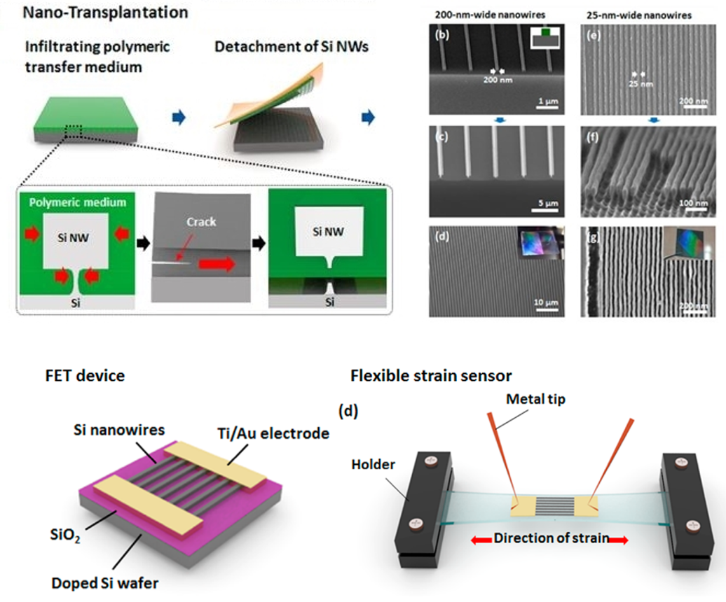
Application to sensor device
Further reading
“Nanotransplantation Printing of Crystallographic-Orientation-controlled Single-Crystalline Nanowire Arrays on Diverse Surfaces” ACS Nano, 2017, 11 (11), pp 11642–11652 Hyeuk Jin Han+, Jae Won Jeong+, Se Ryeun Yang, Cheolgyu Kim, Hyeon Gyun Yoo, Jun-Bo Yoon, Jae Hong Park, Keon Jae Lee, Taek-Soo Kim, Seong-Woong Kim, and Yeon Sik Jung* [Link]
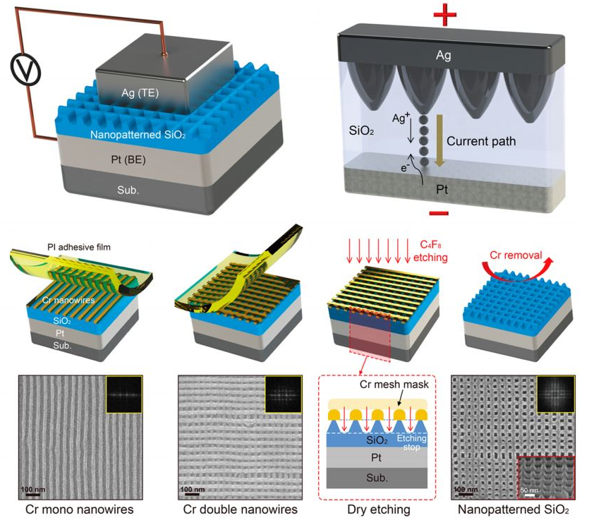
“Reliable Memristive-Switching Memory Devices Enabled by Densely-Packed Silver Nanocone Arrays as Electric-Field Concentrators”ACS Nano, 2016, 10, pp 9478−9488 Byoung Kuk You+, Jong Min Kim+, Daniel J. Joe, Kyounghoon Yang, Youngsoo Shin, Yeon Sik Jung*, and Keon Jae Lee* [Link]